Mosaic Microsystems is proud to support our clients’ business goals with our specialized technology. Our proprietary thin glass solutions address the demanding next generation microelectronics and photonics packaging needs.
Thin Glass
Mosaic’s proprietary thin glass handling solution allows you to temporarily bond thin, flexible glass to a rigid silicon or glass handle wafer to enable manufacture in industry standard processes. We bond thin, smooth glass up to 200 um thick and this is ideal to maintain flatness while depositing thin film structures or otherwise structuring thin glass.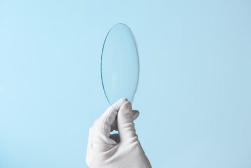
Standard diameters are up to 200 mm, but 300 mm has been recently demonstrated.
See our Standard Products
Thin Glass with Custom Through-Glass Vias (TGV)
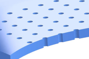 Mosaic will work closely with you to provide custom patterns of TGV on glass wafers temporarily bonded to glass or silicon handle wafers. These products are ideal to address next generation semiconductor packaging, RF, MEMs and micro-fluidics needs.
Our current standard offerings focus on a nominal via diameter of 30 um. Standard glass includes alkali free glass with CTE matching silicon and high purity fused silica, with other options available. See our Standard Products
Please contact us to discuss how we can provide a customized solution to address your TGV needs.
Thin Glass with Custom Filled/Planar Vias
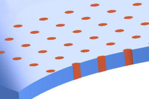
One of the great advantages of Mosaic’s thin glass TGV solutions is the ability to leverage industry standard equipment. Since Mosaic employs a tapered via shape, and bonds to a carrier, the TGV is well-suited to utilize industry standard PVD and plating operations for void free via fill in a blind via format.
The thin, robust bond layer gives conditions to enable good planarity on the bottom of the vias and is also well suited to allow standard CMP processes for overburden removal and planarization. This results in a high quality, fully filled via ready for surface metallization. We look forward to working with you to provide metallized TGV for your integration needs.
Metallized Thin Glass Wafer
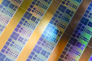
In addition to providing high quality void free TGV, Mosaic’s temporary bond technology gives conditions to enable precision structures to be deposited on the surface. The thin bond layer maintains excellent planarity and flatness enabling fine line spacing exceeding capabilities of both organic and ceramic solutions.
The bond is stable and does not outgas to > 400⁰ C, opening up the parameter space that can be used for top surface metallization. Please contact us to discuss what we can do to enable fabrication of your thin glass designs.