See Mosaic’s article in the latest issue of Chip Scale Review!
Leave a CommentSee the article starting on page 37:
https://chipscalereview.com/wp-content/uploads/flipbook/12/book.html
See the article starting on page 37:
https://chipscalereview.com/wp-content/uploads/flipbook/12/book.html
Mosaic Microsystems, a microelectronics and photonics packaging company providing thin glass substrates and through-glass vias (TGVs) for next-generation products in RF communications, has reported winning a Small Business Technology Transfer (STTR) Phase I award to collaboratively develop ultra-low loss solutions for next-generation radar arrays with the University of Florida. The award is sponsored by the Air Force Research Lab (AFRL) under the AFWERX Agility Prime Open Topic.
Mosaic’s thin glass bonded to a carrier provides characteristics such as low loss, CTE match, stability and cost effectiveness particularly desirable for 5G, as well as MEMs and sensors for the Internet of things (IoT). The proprietary Viaffirm™ temporary bond technology uses innovative approaches to support thin glass substrates during downstream processing. This exciting thin glass handling technology allows the supply chain to process thin glass leveraging the existing infrastructure, thereby unlocking the value that thin glass brings to next generation microelectronics and photonics applications.
Dr. YK Yoon, Professor in the University of Florida’s (UF) Department of Electrical and Computer Engineering (ECE) and Director of the Multidisplinary nano and Microsystems (MnM) Laboratory, is a leader in RF and Microwave technology. His group will lead the effort to provide innovative metaconductor technology to low-loss glass substrates, which can result in order of magnitude reduction in loss performance.
AFWERX Phase I STTR
AFRL and AFWERX have partnered to streamline the Small Business Innovation Research (SBIR) and Small Business Technology Transfer (STTR) process in an attempt to speed up the experience, broaden the pool of potential applicants. Beginning in 2018, and now in 2020, the Air Force has begun offering ‘Special’ SBIR/STTR topics that are faster, leaner and open to a broader range of innovations.
This Phase I STTR award through AFWERX is an exciting program that partners Mosaic with the University of Florida ECE Department and the MnM Lab. Combining Mosaic’s innovative thin glass handling technology, the innovative metaconductor technology developed by Dr. Yoon, and MnM’s RF and mmWave experience will allow the development of radar arrays with a step change in low loss, high gain performance. Establishing highly efficient devices has broad application not only in radar arrays but many other needs across the DoD. Combining both of these innovative technologies will provide a dramatic improvement in size, weight and power performance.
Mosaic Chairman and Chief Executive Officer, Christine Whitman, stated “We are excited to work with the University of Florida to enable important revolutionary higher efficiency devices. This technology will have broad adoption across many defense and commercial markets and is an important part of Mosaic’s roadmap.”
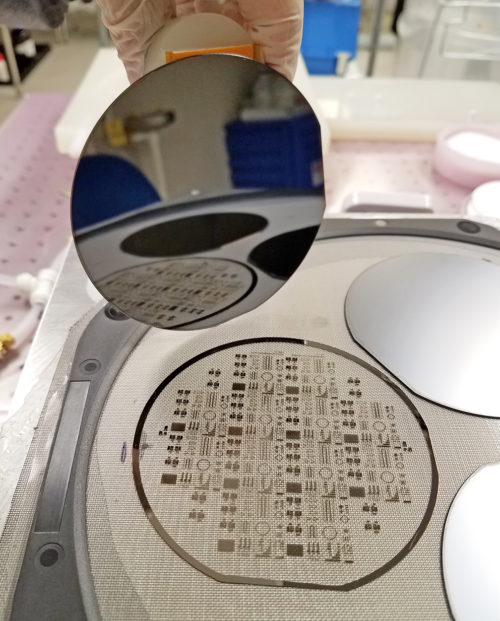 Axus Technology (Axus), a leading global provider of CMP, wafer thinning and wafer surface processing solutions for semiconductor applications, is excited to be working with Mosaic Microsystems to build the supply chain for thin glass and through-glass via (TGV) processing and heterogeneous microelectronic packaging. Overcoming the challenges of handling, thinning, and cleaning <200 um thick wafers cost effectively prior to metallization is a key element in providing a robust, scalable process.
Mosaic’s thin glass solutions provide key performance characteristics such as low loss, CTE match, environmental stability, and cost effectiveness particularly desirable for 5G applications, as well as for MEMs and sensors for the internet of things (IoT). The proprietary Viaffirm™ temporary bond technology, uses innovative approaches to support thin glass substrates during downstream processing. This thin glass handling technology allows the supply chain to leverage the existing infrastructure, thereby unlocking the value that thin glass brings to next generation microelectronics and photonics applications.
Axus’ leading-edge CMP systems and tools help improve the polish performance of thin wafers by utilizing the Axus Crystal carrier, specifically designed for ultra-thin and fragile wafers, along with expert process development from our stellar foundry and development lab. Industry needs for glass wafers are being addressed in a prolific way by the processes that support bonding, debonding, and CMP of thin, fragile substrates.
Dan Trojan, President and CEO of Axus, commented “The development of processes and fragile wafer handling capabilities for thin glass wafers that we’re supporting in our partnership with Mosaic Microsystems is something we’re truly excited about. We believe this development will result in compelling solutions to difficult challenges in this evolving and growing market. We and our customers are already deeply involved in these types of applications, as evidenced by several of our recent new product introductions. These include Crystal wafer carriers, Crystal load stations, and last-but-not-least our new, state-of-the-art CapstoneTM CMP system. We believe that all of these products are the best solutions available in the industry for these types of materials and applications.”
Aric Shorey, Vice President of Business Development at Mosaic Microsystems, commented “We have been very pleased to work with Axus for our CMP and finishing needs and appreciate how they have seamlessly employed Mosaic’s Viaffirm™ temporary bond technology into their processes and been successful in finishing substrates as thin as 100 um from the start.”
###
About Axus Technology
Axus Technology is a recognized industry leader for equipment and process solutions for CMP, wafer thinning and wafer cleaning applications. Axus enables companies of all sizes from startups to high volume manufacturers to test, develop and implement leading-edge solutions, particularly for novel and emerging materials, process integration schemes, products and applications. Equipment solutions include low cost-of-ownership entry-level tools to state-of-the-art high-volume manufacturing systems. Process testing, development, optimization and scaling are supported by our process applications lab and foundry, which includes a full array of process equipment and supporting metrology, staffed by the most experienced team in the industry. For more information, please visit www.axustech.com.
Media Relations Contacts:
Jim Kelly, Vice President of Sales and Marketing| JKelly@axustech.com
About Mosaic Microsystems
Mosaic Microsystems is a microelectronics and photonics packaging company located in Rochester, NY focused on enabling glass and other thin substrates as a platform material for a range of microelectronics and photonics applications including interposers, RF/mmW, MEMS and sensor technologies. We are proud to serve a number of industries and support their business goals with our proprietary technology. For more information, please visit www.mosaicmicro.com.
Media Relations Contacts:
Aric Shorey, VP Business Development| Aric.Shorey@MosaicMicro.com