Posted by NET2ad001 on | Comments Off on Mosaic Microsystems Announces Strategic Leadership Appointments to Drive Next Phase of Innovation and Manufacturing Excellence
Mosaic Microsystems, a pioneering microelectronics and photonics packaging company, today announced strategic leadership changes within its Technology and Manufacturing divisions, signaling a strong commitment to future growth and innovation in advanced substrate solutions.
Effective April 1st, Shelby Nelson, Co-founder and former Chief Technology Officer, has transitioned to the newly created role of Co-founder and Senior Fellow. In this pivotal position, Nelson will continue to contribute her deep technical expertise and vision, which were instrumental in the successful design, development, and launch of Mosaic’s groundbreaking products. Her foundational technology roadmap remains a critical element of the company’s ongoing innovation strategy.
“We extend our deepest gratitude to Shelby Nelson for her visionary leadership and invaluable contributions in establishing Mosaic Microsystems as an industry innovator,” said Christine Whitman, CEO of Mosaic. “Her guidance has been fundamental in taking our initial concepts through to market-leading products, and her continued strategic insights will be crucial as we move forward.”
Building on this strong foundation, David Levy, previously a Senior Scientist at Mosaic, has been promoted to Chief Technology Officer and Vice President of Research & Development. With over 25 years of extensive R&D experience in nano-particle systems, thin film processing, device fabrication, and device physics, Levy will spearhead the advancement of Mosaic’s cutting-edge technical initiatives and drive future innovation.
Further bolstering its operational capabilities, Brian Harding has been elevated from Director of Manufacturing to Vice President of Manufacturing. This promotion recognizes Harding’s significant contributions to scaling Mosaic’s production capabilities and ensuring the delivery of high-quality advanced packaging solutions.
“These strategic leadership appointments underscore Mosaic’s proactive approach to positioning the company for its next phase of expansion,” added Whitman. “As the demand for advanced glass substrates continues to grow within the microelectronics packaging landscape, we are confident that this strengthened leadership team will accelerate our innovation and manufacturing excellence.”
About Mosaic Microsystems
Mosaic Microsystems is a Rochester, NY-based microelectronics and photonics packaging company specializing in enabling glass and other thin substrates as a transformative platform material for a diverse range of applications. These include interposers, RF/mm-Wave technology, MEMS, and advanced sensor technologies. Committed to serving various industries, Mosaic leverages its proprietary technology to empower customers in achieving their critical business objectives. For more information, please visit www.mosaicmicro.com.
Posted by NET2ad001 on | Comments Off on Entrepreneur of the Year Shelby F. Nelson, PhD
Shelby F. Nelson, PhD has been selected as the 2024 Entrepreneur of the Year by the Rochester Section of the American Chemical Society.
This award recognizes Dr. Nelson’s co-founding of Mosaic Microsystems and developing and commercializing innovative glass packaging technology for integration of microelectronic and photonic chips.
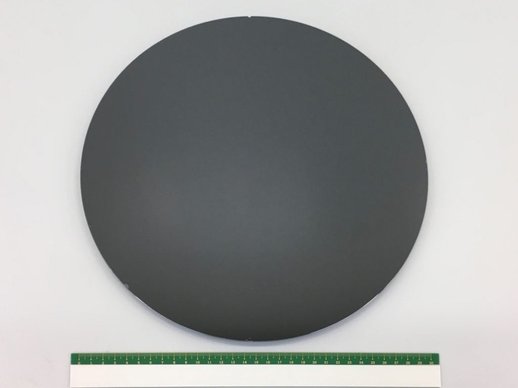
Mosaic’s proprietary glass handling technology allows temporary bonding of thin, flexible glass to a rigid handle wafer, to enable high-yield manufacturing of electrical and optical traces and circuits, leveraging industry standard processes normally used for silicon. This technology works with glass even below 100 microns thick.
Mosaic wants engineers who are involved in RF, computing, integrated photonics, and biomedical devices to know the benefits of glass for advanced semiconductor packaging.Glass can be thought of as a very high-performance printed circuit board (PCB) — enabling cutting-edge applications to meet their challenging targets.
Mosaic’s early understanding of the value of glass has been underscored by recent announcements by companies like Intel and Samsung of a drive to incorporate glass in their advanced packaging. Mosaic’s special expertise is in the production of thin glass packaging solutions, with successful (high yield) handling of the floppy and transparent material through the many steps required to produce finished packages.
Mosaic is prototyping thin glass with multi-layer interconnects, along with copper-filled through-glass vias connecting front to back of the glass, and is rapidly moving these to production for both defense and commercial industries.
Posted by David Levy on | Comments Off on Mosaic Awarded $1 Million from DBX Challenge
Mosaic Microsystems LLC proudly announces its success in winning a $1.0 million award as one of the competitors in the Defense Business Accelerator (DBX) Microelectronics Challenge. This strategic initiative, aimed at revolutionizing how the Department of Defense catalyzes commercial technology development, is both a significant milestone for Mosaic Microsystems and the start of an interesting new era in the broader defense technology landscape.
Mosaic Microsystems emerged as a finalist from a pool of over 270 applications, presenting their “Thin Glass Substrates for Advanced Microelectronics Packaging” solution at the Defense TechConnect Innovation Summit on November 28. A distinguished panel of industry, government, and investment experts evaluated the pitches, ultimately awarding seven winners a combined total of $10 million in funding.The DBX Microelectronics Challenge, a new program fostering innovation within the Department of Defense, serves as a catalyst for industrial base growth and private investment stimulation. By prioritizing commercial technology development, the challenge aims to expedite solution development and enhance the longevity of suppliers, ushering in a new era of collaboration between industry, government, and investment sectors. https://www.uspae.org/wp-content/uploads/2023/12/231204-USPAE-Release-DBX-Awardees.pdf
The DBX challenge is a collaborative effort, merging the electronics industry expertise of the U.S. Partnership for Assured Electronics (USPAE) and the Department of Defense’s Manufacturing, Capability Expansion, and Investment Prioritization Directorate (MCEIP). Tactical support from Advanced Technology International (ATI), specifically the TechConnect division, further bolsters the challenge’s impact on the selected winners and the broader community.
Mosaic Microsystems showcased their innovative thin glass technology for advanced microelectronics packaging. The applications span various domains, including RF, compute, integrated photonics, and biomedical devices. Mosaic is prototyping thin glass with multi-layer interconnects, along with copper-filled through-glass vias connecting front to back of the glass, and will rapidly move these to production for both defense and commercial industries.
“We are pleased to have been selected for this prestigious award,” says Christine Whitman, CEO of Mosaic Microsystems. “The Defense Business Accelerator recognition validates our business strategy for expansion and underscores the critical role of Mosaic’s glass technology.”
Posted by David Levy on | Comments Off on Mosaic Microsystems co-founder interviewed about recent DoD contract
Mosaic Microsystems co-founder, Shelby F. Nelson, is interviewed about Mosaic’s recent DoD contract and how it will help Mosaic connect chips to photonics and the outside world.
Posted by David Levy on | Comments Off on Rochester Business Journal spotlights Mosaic for recent DOD award
RBJ spotlights Mosaic for a recent DOD award using its cutting edge glass interposers for an advanced high speed photonics packaging solution. Read the full article here.
Posted by David Levy on | Comments Off on Brittany Hedrick Joins Mosaic Microsystems as Integration Engineer
Mosaic Microsystems proudly announces the addition of Brittany Hedrick as Senior Engineering Manager. Brittany brings a wealth of experience in silicon photonics integration, wafer finishing, and packaging assembly, which will propel Mosaic’s innovative glass interposer solutions to new heights. Mosaic Microsystems, situated within the Eastman Business Park in Rochester, NY, is renowned for its rapid-paced application of thin glass towards replacing long standing silicon packaging solutions.
Brittany Hedrick joins Mosaic Microsystems from the role of Si Photonics Integration Engineer, with a robust professional background earned over the course of 12 years in the industry. She brings her expertise in a variety of fields, including 2.5D/3D packaging development, Si Photonics Post Fab enablement, and experience in the fabrication of both silicon and glass interposers. From her start as a Process Development Engineer to her role as Lead Post Fab Photonics Integrator, she has acquired a breadth of experience to apply at Mosaic.
“We are thrilled to welcome Brittany Hedrick to our team at Mosaic Microsystems,” said Shelby Nelson CTO of Mosaic Microsystems.
As the Senior Engineering Manager at Mosaic, Brittany will play a pivotal role in shaping the company’s future. Her responsibilities span from overseeing management of new projects to development of new glass packaging solutions. Brittany’s expertise will be instrumental in harmonizing processes, driving innovations in production quality, and addressing the diverse technical challenges presented by Mosaic’s clientele – which ranges from commercial customers to government contracts.
Posted by David Levy on | Comments Off on Mosaic Microsystems Co-Founder Shelby Nelson to speak at iNEMI/Zestron workshop
Shelby F. Nelson, Mosaic Microsystems, will present, “Glass Substrate for Packaging” at the iNEMI/ZESTRON workshop, Advanced Packaging and Its Impact on mmWave Applications, November 7 in Manassas, Virginia. This full-day workshop brings together industry-based and academic researchers to talk about the challenges of advanced packaging and its intersection with high-frequency (mmWave) materials. We will also share highlights from the NIST-sponsored 5G/6G mmWave Materials and Electrical Test Technology Roadmap (5G/6G MAESTRO). Get additional details and make plans to join us in person or virtually.
Posted by David Levy on | Comments Off on Mosaic Microsystems’ Co-Founder Paul Ballentine Guests on 3D InCites podcast
Mosaic Microsystems co-founder Paul Ballentine and 3D InCites’ Francoise von Trapp discuss how Mosaic is developing thin glass substrates and interposers for advanced packaging in their Rochester, New York fab as one of the only domestic sources.
Posted by David Levy on | Comments Off on DoD Awards Contract to Mosaic Microsystems
DoD Awards Contract to Mosaic Microsystems to work with AIM Photonics on cutting-edge glass-based electronic and photonic interposers
Mosaic Microsystems, a pioneering leader in advanced microelectronics glass packaging technology, is delighted to announce the successful award of a Phase II Small Business Innovation Research (SBIR) contract by the Department of Defense (DoD). This award reflects Mosaic Microsystems’ commitment to pushing the boundaries of innovation and its dedication to enhancing national defense capabilities.
Under this Phase II SBIR effort, Mosaic Microsystems will develop ultra-thin glass interposers with through-glass via (TGV) technology. These cutting-edge interposers will serve as the foundation for a high-speed packaging solution designed for analog and digital electronics and photonics. As part of this transformative initiative, in collaboration with the American Institute for Manufacturing Integrated Photonics (AIM Photonics), Mosaic Microsystems’ will demonstrate the integration of fiber optics, waveguides, and photonic integrated circuits (PICs) with glass.
Advanced application-specific integrated circuit (ASIC) or PIC-based systems currently rely on a silicon (Si) substrate for the electronic interposer or electronic and photonic interposer (respectively) and an organic laminate substrate for RF signals, power, and control. Mosaic Microsystems’ effort will leverage the capabilities of AIM Photonics’ Test, Assembly and Packaging (TAP) facility to develop photonics-enabled glass interposers. Mosaic’s glass interposers promise greater efficiency, superior electrical and thermal isolation, and more compact packaging solutions compared to the conventional packages.
This innovative approach will apply not only to defense technology but also to commercial applications. By introducing thin glass photonic interposers, Mosaic Microsystems seeks to demonstrate substantial cost savings, reduced size and weight, and enhanced overall performance over current solutions. These advantages are expected to have far-reaching implications for next-generation digital communications and have the potential to shape the future of 5G and ‘Next G’ technologies.
“This DoD SBIR Phase II contract supports our team’s ability to drive technological innovations in the important area of photonics packaging,” said Shelby Nelson, Chief Technology Officer and Co-Founder at Mosaic Microsystems. “We are thrilled to collaborate with AIM Photonics TAP on this venture, as we help build the future of electronics, photonics, and communications technologies.”
About Mosaic Microsystems:
Mosaic Microsystems is a microelectronics and photonics packaging company located in Rochester, NY focused on enabling glass and other thin substrates as a platform material for a range of microelectronics and photonics applications including interposers, RF/mmW, MEMS and sensor technologies. We are proud to serve a number of industries and support their business goals with our proprietary technology.
For media inquiries or more information about Mosaic Microsystems and its pioneering work, please contact: Chris Mann, Vice President of Business Development, Chris.Mann@Mosaicmicro.com, 585-298-0198.
About AIM Photonics:
The American Institute for Manufacturing Integrated Photonics (AIM Photonics) is one of nine Manufacturing Innovation Institutes established and managed by the U.S. Department of Defense to advance new technology and capabilities into products and systems that help secure national defense and economic priorities. AIM Photonics enables current and future photonics technologies by integrating photonic components on a silicon wafer fabricated using a standard silicon foundry process. AIM Photonics’ goal is to help U.S. companies—both small and large—develop innovative products and services by providing them with technology on-ramps and access to strategic U.S. government, industry, and academic communities. AIM Photonic offers prototyping services through the Albany NanoTech Complex, the most advanced publicly owned 300 mm wafer R&D facility in the world, and a state-of-the-art 300 mm test, assembly, and packaging (TAP) facility in Rochester, New York, which provides advanced wafer-level and die-level test and assembly for electronic and photonic packaging. More information can be found at www.aimphotonics.com.